


Inspection Techniques Play in PCB Board Assembly Manufacturing?
The PCB board assembly manufacturing process is essential to the performance and functionality of electronic devices. A well-executed inspection process can identify and eliminate defects that might otherwise lead to costly product recalls, customer dissatisfaction, and damage to a company’s reputation. Moreover, it can foster customer trust and loyalty by delivering products that meet high standards for quality and reliability. In order to ensure the quality of PCB boards, inspection services should be implemented at every stage of production. This can help prevent costly errors and ensure compliance with industry regulations.
In the earliest stages of a PCB development project, visual inspection is a vital tool. This method allows inspectors to detect defects early, reducing the likelihood of costly mistakes that might go unnoticed in later production phases. It also helps to reduce waste and ensures that the final product meets its specifications.
To conduct a visual inspection, an experienced technician examines the pcb board assembly manufacturing with a magnifying lens to spot any glaring errors. This can be a time-consuming process, but it is highly effective in uncovering flaws and imperfections that might have gone undetected by automated inspection systems. However, it is important to ensure that the fabricator you choose has the necessary expertise and equipment to perform this inspection effectively.
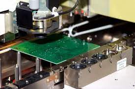
Automated optical inspection (AOI) is another common PCB inspection method. This system uses a series of cameras to capture images of the finished circuit board and compare them to an ideal model. Any inconsistencies can reveal defects such as solder shorts, open connections, and misalignments. AOI systems typically work at faster speeds than manual inspections, making them suitable for large batches of PCBs.
What Role Do Inspection Techniques Play in PCB Board Assembly Manufacturing?
X-ray inspection is another fast and reliable method for identifying defects in PCBs. This technology works by analyzing the atomic weight of various materials in a given PCB. Heavier elements, such as solder and other metals, are easier to see in x-ray images, while lighter components are harder to discern. This can help inspectors locate problems such as faulty soldering, pin-hole fills, and other issues that might not be visible to the naked eye.
In addition to these automated inspection methods, manual inspections are still commonly used. In particular, this type of inspection can be useful for identifying issues with complex SMDs that might be difficult to recognize using a camera or AOI machine. Manual inspections can also identify more subtle defects such as dirt, scratches, and dents that may have affected the quality of the circuit board.
Inspection techniques allow for the early detection of faults and defects in the PCB assembly process. By identifying issues such as soldering defects, component misalignment, or trace damage at an early stage, manufacturers can prevent these problems from escalating into more significant issues that could compromise the functionality of the final product. Early detection is crucial for minimizing waste and reducing the need for costly rework or scrap.


+ There are no comments
Add yours