
What is the Difference Between Single-Layer and Multi-Layer HDI PCB?
HDI PCBs (High-Density Interconnector PCBs) are critical for creating advanced electronic devices, offering enhanced performance, reduced size, and increased functionality. These boards are designed with a focus on compactness and high-density interconnects, allowing for greater miniaturization of electronic components. HDI PCBs can be classified into different types, including single-layer and multi-layer designs. Both of these designs serve different purposes, and understanding their differences is essential for selecting the right PCB for specific applications. In this article, we will explore the key differences between single-layer and multi-layer HDI PCBs.
Single-Layer HDI PCB: Simplicity and Cost Efficiency
A single-layer HDI PCB, as the name suggests, consists of just one layer of conductive material. This layer supports the circuitry and is typically built with microvias to connect traces to other components. Single-layer HDI PCBs are simpler and more cost-effective compared to multi-layer boards, making them ideal for less complex electronic devices where the routing and interconnection requirements are relatively straightforward.
In single-layer hdi pcb, the microvias connect the components within a single layer, which is often sufficient for basic applications that do not require extensive layer-to-layer connections. These types of PCBs are commonly used in devices such as smartphones, wearable gadgets, and other compact electronic products. The primary benefit of single-layer HDI PCBs is their reduced manufacturing cost, as the design involves fewer materials and simpler processes compared to multi-layer boards.
Additionally, single-layer HDI PCBs tend to have faster production times, making them ideal for industries where quick turnaround and cost are priorities. However, they are limited in their complexity and cannot handle the same level of signal routing or component density as multi-layer designs.
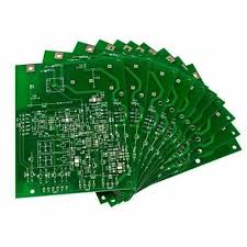
Multi-Layer HDI PCB: Complexity and Enhanced Functionality
On the other hand, multi-layer HDI PCBs consist of several layers of conductive material, stacked together and interconnected through microvias. These multiple layers allow for more complex and dense routing, enabling the PCB to accommodate more components and features within a smaller footprint. Multi-layer HDI PCBs are often used in high-performance applications where space constraints, functionality, and performance requirements demand more intricate and denser designs.
The primary advantage of multi-layer HDI PCBs is their ability to handle complex circuits with multiple signal layers. They can interconnect different layers using microvias and blind or buried vias, making it possible to route signals in various directions without compromising performance. This ability to create more intricate layer-to-layer connections is crucial in devices such as advanced smartphones, tablets, automotive electronics, and medical devices, where higher functionality is necessary.
The increased number of layers allows designers to create more compact and reliable electronic products. However, the complexity of multi-layer HDI PCBs results in higher manufacturing costs and longer production times, as more materials and advanced techniques are involved in their creation. These factors must be considered when choosing between single-layer and multi-layer designs.
Key Differences Between Single-Layer and Multi-Layer HDI PCB
1. Complexity
The most significant difference between single-layer and multi-layer HDI PCBs is their complexity. Single-layer HDI PCBs are simple, with one conductive layer, while multi-layer HDI PCBs are more complex, consisting of multiple stacked layers. The design and production process for multi-layer boards requires more advanced techniques, including precise layer alignment and interlayer via creation.
2. Routing Density
Multi-layer HDI PCBs offer greater routing density than single-layer boards. With multiple layers available, designers can route more complex circuits and integrate more components. This makes multi-layer HDI PCBs ideal for devices that require high functionality in a compact form factor.
3. Size and Miniaturization
While single-layer HDI PCBs are already compact, multi-layer HDI PCBs offer even greater potential for miniaturization. The use of multiple layers allows for more efficient use of space, making multi-layer HDI PCBs ideal for applications where minimizing size while maintaining performance is critical.
4. Cost and Production Time
Single-layer HDI PCBs are less expensive to manufacture and quicker to produce due to their simplicity. In contrast, multi-layer HDI PCBs require more advanced manufacturing processes and materials, which results in higher costs and longer production times.
5. Applications
Single-layer HDI PCBs are suitable for simpler electronic devices with less complex interconnections, such as wearables or basic consumer electronics. Multi-layer HDI PCBs, however, are essential for high-performance applications like smartphones, medical devices, and automotive electronics, where more intricate and dense circuitry is necessary.
Conclusion
Both single-layer and multi-layer HDI PCBs have their advantages, and the choice between the two depends on the complexity, size, and performance requirements of the device in question. Single-layer HDI PCBs offer simplicity, cost-efficiency, and quick production times, making them ideal for less complex applications. Multi-layer HDI PCBs, however, are designed for more sophisticated electronics that require increased functionality, routing density, and miniaturization. Understanding the differences between these two types of HDI PCBs is crucial for selecting the right PCB for any electronic project.

+ There are no comments
Add yours